


In order to efficiently and quickly fulfill your order, it is necessary to adhere to the following requirements:
Download the input documentation here.
|
Width |
50 – 350 mm |
|
Lenght |
50 – 450 mm |
|
Thickness |
0,4 – 2,6 mm (the possibility of using thinner boards should be discussed) |
By the term 'cross-section,' we mean the matrix of X x Y individual board patterns, which are typically bounded by the technological context.
For PCBs, it is crucial that their longitudinal edges are parallel, and within one production series, the width tolerance should be a maximum of 0.5mm! Otherwise, there is an increased risk of board (cross-section) damage during production or potential production delays.
Regarding rigidity or board deflection, especially for problematic boards (weak boards, narrow bridges on the cross-section, excessively deep-milled grooves, Teflon boards, etc.), we recommend consultation for each specific case.
The minimum distance from the edge of the soldering pad to the edge of a single-sided PCB is 3 mm. For double-sided PCBs, a 10mm margin is required. If the soldering pads are closer to the PCB edge, the board must have a technological edge. If this is not the case, components on the edge of the board must be assembled separately, resulting in delays and increased costs for such assembled boards.
Technological Holes:
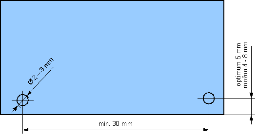
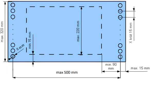
For securing the PCB (individual boards or cross-section) in the placement machine, it is advisable for the technological environment (the board) to have ideally 5 mm (range 4 – 8 mm) from its lower edge two holes with a diameter of 3 mm (by agreement, 2 – 4 mm is possible - see the image below). For a double-sided board, it is recommended to add securing points on both sides. If this is not the case, the risk of inaccurate placement increases.
Technological Marks:
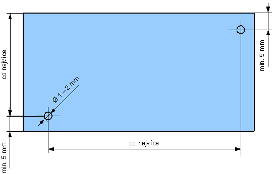
For precise PCB alignment before printing or assembly, it is advisable for the board to have at least two alignment marks. These could be circular discs with a diameter of approximately 1 - 2 mm placed on the board diagonally (asymmetrically) and as far apart from each other as possible, with a surface matching the solder pad surface (uncovered by solder mask). These marks must be located at least 5 mm from the longitudinal edge of the board (see the image below). Any shape other than a circular shape for alignment discs should be discussed in advance. It is essential that within a radius of at least 3 mm around the alignment point, there are no solder pads, markings, etc., on the board. If the marks on the board (cross-section) are absent or of low quality, the risk of inaccurate alignment/board assembly increases.
Wave Soldering:
When considering wave soldering, it is advisable not to make boards (cross-sections) - especially those with lower rigidity - too wide to prevent them from bending during the wave soldering process. The board design should account for the possibility of wave soldering, and components with a large number of pins (e.g., connectors) should be oriented in one direction, assuming the board's movement through the wave (longitudinally with the longer side of the cross-section) to prevent short circuits after passing through the wave.
Components:
Following prior consultation, we offer you the option to use common components from our inventory. For other components, you may provide them yourself, or we can arrange their procurement from our suppliers. If you choose to provide the components yourself, you must adhere to the following rules:
Failure to comply with these rules may result in increased component consumption, poor assembly quality, or improper component soldering.
Production Documentation:
The documentation you provide must include:
In the case of poor documentation, errors may occur in the execution of the order or unnecessary delays. The provided documentation may also include component coordinates, orientation angles, and other supplementary or clarifying information.
Templates for Printing:
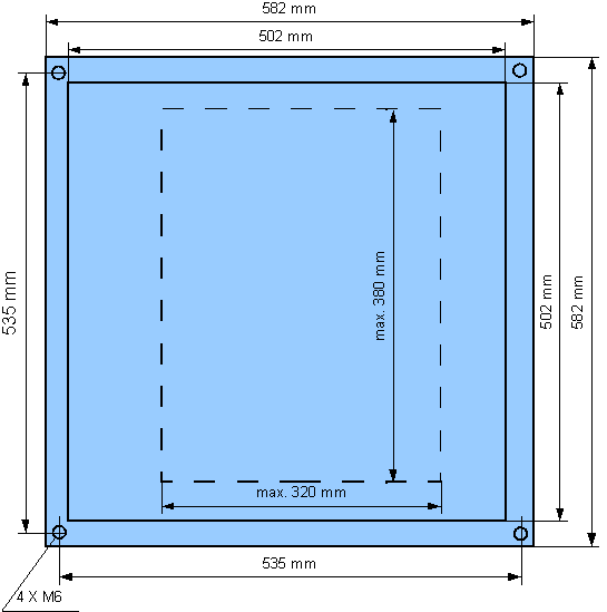
Solder paste or adhesive printing for SMD components can be done either with the DEK machine or the manual UNIPRINT device. The advantage of using the DEK machine for paste application is its larger area and precision in paste application. The manual UNIPRINT dispenser is suitable for sample production and smaller runs. The images show the maximum printing area for SMD pads (do not confuse with board or cross-section dimensions, which may be larger).
DEK Template (ver. 1)
DEK Template (ver. 2)
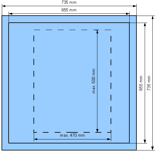
The DEK template should have two depressions on the bottom side (not holes!), preferably in a circular shape with a diameter matching the diameter of the alignment marks on the board, positioned at points corresponding to the alignment points on the board. If the template lacks these depressions, it may lead to inaccurate printing or prolonged printing time.
UNIPRINT Template
The thickness of the template, or the method of template production, is primarily chosen based on the type of components being placed.
We recommend consulting with us regarding the template thickness before its production.
Would you like to consult? Call +420 603 477 901
![]()
Podnikatelská 553
190 11 Praha 9 - Běchovice
Česká republika
© Copyright 2017 MICRO CZECH REPUBLIC, s.r.o.
![]()